
From sheet to stack, new nanostructures promise a leap forward for advanced electronics
[ad_1]
(Nanowerk News) Researchers at Tokyo Metropolitan University have successfully developed multilayered nanostructures of transition metal dichalcogenides (TMDCs) that form in-plane junctions. By growing molybdenum disulfide structures in layers from the edges of niobium-doped molybdenum disulfide fractions, the scientists created a strong, bonded planar heterostructure.
They demonstrated that this structure could be used to fabricate new tunnel field-effect transistors (TFETs), which are ultra-low-power-consuming components in integrated circuits.
This research has been published in ACS nano (“Multilayer In-Plane Heterostructures Based on Transition Metal Dichalcogenides for Advanced Electronics”).
The field-effect transistor (FET) is a critical component in nearly all digital circuits, controlling the flow of current depending on the applied voltage. Although metal oxide semiconductor FETs (MOSFETs) currently dominate the market, researchers are looking to next-generation materials to build increasingly efficient and compact devices that use less power. Tunneling FETs (TFETs) are a promising alternative, relying on quantum tunneling, which allows electrons to pass through seemingly impassable barriers due to quantum mechanical effects. However, developing a scalable deployment of this technology remains a challenge.
Under the guidance of Associate Professor Yasumitsu Miyata, the team at Tokyo Metropolitan University focused on fabricating nanostructures from transition metal dichalcogenides (TMDCs), which are mixtures of transition metals and group 16 elements. TMDCs are ideal candidates for TFETs due to their unique properties. Researchers have achieved remarkable success in piecing together layers of one-atom-thick crystalline TMDC sheets, and they have now turned their focus to the multi-layered structure of TMDC.
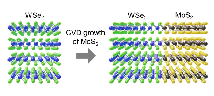
Using chemical vapor deposition (CVD), the team demonstrated that they could grow TMDCs that differ from the edges of stacked crystal planes fixed to a substrate, creating in-plane couplings with multiple layers. Previous work on TMDC junctions mainly involved monolayers stacked on top of each other, as achieving the high concentrations of holes and electrons required for TFETs proved elusive with in-plane junctions.
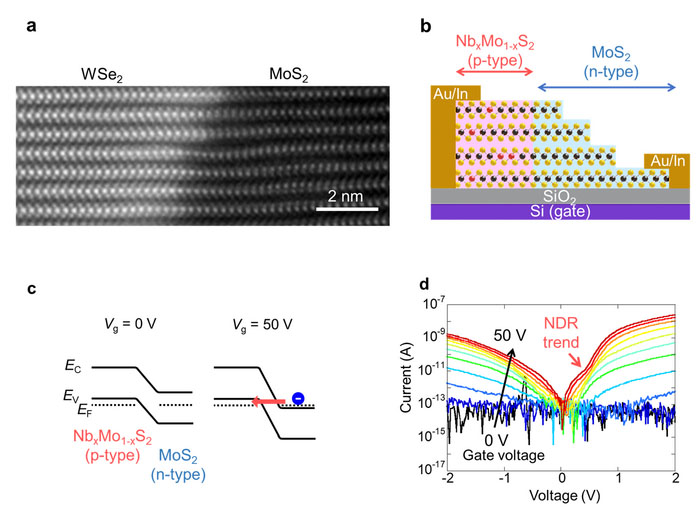
After validating their technique using molybdenum disulfide grown from tungsten selenide, the researchers turned to molybdenum disulfide doped with niobium, a p-type semiconductor. By growing a multi-layered structure from an undoped molybdenum disulfide, an n-type semiconductor, the team created thick pn junctions between TMDCs with very high carrier concentrations. They also found that the junctions exhibit a negative differential resistance trend (NDR), a key feature of tunneling and a critical first step for incorporating these nanomaterials into TFETs.
In particular, the team method is scalable over large areas, making it suitable for circuit building. These innovative developments hold great promise for the future of modern electronics, and it is anticipated these innovative materials will find their way into a wide variety of applications.
[ad_2]
Source link