
MIT engineers “grow” atom-thin transistors on top of computers
CAMBRIDGE, MA — Emerging AI applications, such as chatbots that generate natural human language, are demanding denser and more powerful computer chips. But semiconductor chips have traditionally been made with bulk materials, which are 3D grid structures, so stacking multiple layers of transistors to create a tighter integration is extremely difficult.
CAMBRIDGE, MA — Emerging AI applications, such as chatbots that generate natural human language, are demanding denser and more powerful computer chips. But semiconductor chips have traditionally been made with bulk materials, which are 3D grid structures, so stacking multiple layers of transistors to create a tighter integration is extremely difficult.


However, semiconductor transistors made of ultrathin 2D materials, each only three atoms thick, can be stacked to make more powerful chips. To this end, MIT researchers have now demonstrated a new technology that can effectively and efficiently “grow” layers of 2D transition metal dichalcogenide (TMD) materials directly on top of fully fabricated silicon chips to enable denser integration.
Growing 2D materials directly onto CMOS silicon wafers has posed a major challenge as the process usually requires temperatures around 600 degrees Celsius, while transistors and silicon circuits can be damaged when heated above 400 degrees. Now, an interdisciplinary team of MIT researchers has developed a low-temperature growth process that doesn’t damage the chip. This technology allows 2D semiconductor transistors to be integrated directly onto standard silicon circuits.
In the past, researchers have grown 2D material elsewhere and then transferred it onto a chip or wafer. This often causes imperfections that hinder the performance of devices and final circuits. Also, transferring material smoothly becomes very difficult at the wafer scale. Instead, the new process grows a smooth, highly uniform layer across an 8-inch wafer.
This new technology is also able to significantly reduce the time needed to grow these materials. While the previous approach required more than one day to grow a single layer of 2D material, the new approach can grow a uniform layer of TMD material in less than one hour across an 8-inch wafer.
Due to its fast speed and high uniformity, this new technology allows researchers to successfully integrate layers of 2D materials onto much larger surfaces than has been previously demonstrated. This makes their method more suitable for use in commercial applications, where wafers that are 8 inches or larger are key.
“Using 2D materials is a powerful way to increase the density of integrated circuits. What we do is like building a multi-storey building. If you only have one floor, which is a conventional case, it won’t accommodate many people. But with more floors, the building will accommodate more people which can make amazing new things possible. Thanks to the heterogeneous integration that we are working on, we have silicon as the first floor and then we can have many floors of 2D materials integrated directly on top of it,” said Jiadi Zhu, an electrical engineering and computer science graduate student and co-lead author of the paper on the new technique. This.
Zhu co-authored the paper with co-lead-author Ji-Hoon Park, MIT postdoc; author of the correspondence Jing Kong, professor of electrical engineering and computer science (EECS) and member of the Research Laboratory for Electronics; and Tomás Palacios, EECS professor and director of the Microsystem Technology Laboratory (MTL); as well as others at MIT, MIT Lincoln Laboratory, Oak Ridge National Laboratory, and Ericsson Research. This paper appears today in Natural Nanotechnology.
Sleek material with great potential
The 2D material the researchers focused on, molybdenum disulfide, is flexible, transparent, and exhibits strong electronic and photonic properties making it ideal for semiconductor transistors. It consists of a layer of one molybdenum atom sandwiched between two sulfide atoms.
Growing molybdenum disulfide thin films on surfaces with good uniformity is often accomplished by a process known as metal-organic chemical vapor deposition (MOCVD). Molybdenum hexacarbonyl and diethylene sulfur, two organic chemical compounds containing molybdenum and sulfur atoms, are vaporized and heated in a reaction chamber, where they “break down” into smaller molecules. Then they link through chemical reactions to form molybdenum disulfide chains on the surface.
But the breakdown of these molybdenum and sulfur compounds, known as precursors, requires temperatures above 550 degrees Celsius, whereas silicon circuits begin to degrade when temperatures exceed 400 degrees.
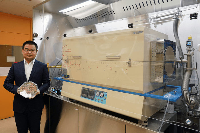
So the researchers started by thinking outside the box — they designed and built an entirely new furnace for metal-organic chemical vapor deposition processes.
The oven consists of two chambers, a low temperature area at the front, where the silicon wafers are placed, and a high temperature area at the back. The vaporized molybdenum and sulfur precursors are pumped into the furnace. Molybdenum remains in a low-temperature region, where the temperature is kept below 400 degrees Celsius — hot enough to decompose molybdenum precursors but not so hot that it damages silicon chips.
The sulfur precursor flows into a region of high temperature, where it decomposes. It then flows back to a lower temperature region, where the chemical reaction to grow molybdenum disulfide on the wafer surface takes place.
“You can think about spoilage like making black pepper — you have whole peppercorns and you grind them into a powder. So, we crush and grind the pepper in the high-temperature region, then the powder flows back to the low-temperature region,” explained Zhu.
Faster growth and better uniformity
One problem with this process is that silicon circuits usually have aluminum or copper as a top layer so that the chip can be connected to a package or carrier before being attached to the printed circuit board. But sulfur causes these metals to become sulfur, in the same way some metals rust when exposed to oxygen, which impairs their conductivity. The researchers prevented sulfurization by first depositing a very thin layer of passivation material over the chip. Then later they can open up the passivation layer to make the connection.
They also placed the silicon wafers into the low temperature area of the furnace vertically instead of horizontally. By placing them vertically, neither edge gets too close to high-temperature areas, so no part of the wafer is damaged by heat. Plus, the molybdenum and sulfur gas molecules swirl as they hit the vertical chip, instead of flowing over a horizontal surface. This circulation effect enhances the growth of molybdenum disulfide and results in better material uniformity.
As well as producing a more uniform coating, their method is also much faster than other MOCVD processes. They can grow layers in less than an hour, while normally the MOCVD growing process takes at least a full day.
Using the state-of-the-art MIT.Nano facility, they were able to demonstrate high uniformity and material quality across an 8-inch silicon wafer, which is critical for industrial applications that require larger wafers.
“By shortening the growth time, the process is much more efficient and can be more easily integrated into industrial fabrication. Plus, it is a silicon-compatible low-temperature process, which could be useful for pushing 2D materials further into the semiconductor industry,” said Zhu.
In the future, the researchers want to refine their technique and use it to grow multiple layers of 2D transistors. Additionally, they want to explore the use of the low-temperature growing process for flexible surfaces, such as polymers, textiles or even paper. This could enable the integration of semiconductors into everyday objects such as clothing or notebooks.
###
This work was partially funded by the MIT Institute for Soldier Nanotechnologies, the National Science Foundation Center for Integrated Quantum Materials, Ericsson, MITER, the US Army Research Office, and the US Department of Energy. This project also received support from TSMC University Shuttle.
Journal
Natural Nanotechnology
DOI
10.1038/s41565-023-01375-6