
Controlling the shape of quantum dots with nanofaceting
[ad_1]
(Nanowerk News) A new method for controlling the shape of quantum dots could make technologies that support our everyday lives more stable and more efficient, scientists claim.
The process provides the industry with opportunities to optimize optoelectronics, energy harvesting, photonics and biomedical imaging technologies, according to a Cardiff University-led team.
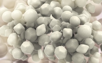
Their study, was funded by the Engineering and Physical Science Research Council (EPSRC) and published in Nano Letters (“Evolution of Local Structural Motifs in Colloidal Quantum Dot Nanocrystals Leading to Nanofaceting”), uses a process called nanofaceting – the formation of tiny, flat surfaces on nanoparticles – to manipulate quantum dots into various shapes called nanocrystals.
From cubic and olive-like structures to complex truncated octahedra, an international research team says these nanocrystals have unique optical and electronic properties, which can be used in a wide variety of technologies.
Dr Bo Hou, Senior Lecturer in Cardiff University’s School of Physics and Astronomy who led the research, said: “The quantum dot has the potential to revolutionize a number of industries because of the theoretical efficiency it offers without limits. Our study represents a significant step forward in the adoption of quantum dot technology in various energy and lighting industry applications.
“With further development, we can envision the truncated octahedra we produce being used to harvest energy in solar cells, increasing efficiencies beyond current technology capabilities which are around 33%. Similarly, our nanocrystals can be used for biomedical imaging, where current inefficiencies and instability limit their use in diagnosis and drug delivery.”
“So this technology is really the future and our work to play a role in accelerating its adoption is very exciting.”
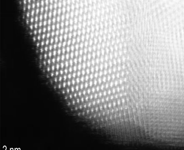
Working in a state-of-the-art laboratory at Cardiff University’s new Translational Research Hub (TRH), the team grows compound semiconductor nanocrystals in solvents and monitors their development in real time using computer simulations and powerful microscopy technology.
Dr Hou added: “Cultivating semiconductors in solvents is our top choice due to its low carbon footprint, higher yield potential and economic benefits when compared to the high temperatures and vacuum conditions required in traditional production.
“It also means we can study the effect of solvent polarity on the shape of the nanocrystals, which could provide a means of stabilizing polar surfaces with further research.”
The team is currently developing a low-carbon footprint LED and image sensor that will enable industries to incorporate quantum dot nanocrystals into their technology for increased resolution and energy efficiency.
[ad_2]
Source link