
Disabled master
[ad_1]
(Nanowerk News) Bruno Schuler and his young team are embarking on an ambitious research project: He will selectively generate defects in atom-thin semiconductor layers and attempt to measure and control their quantum properties with simultaneous picosecond temporal resolution and atomic precision. The resulting insights are expected to build fundamental knowledge for future quantum computers.
The term molybdenum disulfide may sound familiar to some car drivers and mechanics. No wonder: the substance, discovered by US chemist Alfred Sonntag in the 1940s, is still used today as a high-performance lubricant in engines and turbines, but also for bolts and screws. This is due to the special chemical structure of these solids, in which the individual layers of the material are easily displaced relative to each other.
However, molybdenum disulfide (chemically MoS2) not only lubricates well, but also makes it possible to peel off single atomic layers of this material or grow it synthetically on a wafer scale. Controlled isolation of MoS2 monolayers were achieved only a few years ago, but are already considered a material science breakthrough with enormous technological potential. The Empa team now wants to work with precisely this class of materials.
The layered structure of individual layers of atoms makes this material attractive to physicists seeking the basis for next-generation nanocomputers. MoS2 – and its chemical relatives called transition metal dichalcogenides (TMDs) – are one of the main “shooting stars” in a wide variety of two-dimensional (2D) materials.
TMDs are 2D semiconductors and have a direct band gap, but only as a single layer, making them very attractive for miniature integrated circuits or optical detectors. The strong quantum mechanical properties of 2D materials are also being intensively explored for use in quantum metrology, quantum cryptography, and quantum information technology.
But it’s not just the base materials that matter, but in particular the ability to manage defects there: Analogous to “classical” semiconductor chemical doping in integrated circuits or foreign ions in solid-state lasers, atomic defects are “like the icing on the cake,” especially in 2D materials, Schuler said.
Atomic-thin quantum computers?
Empa researchers wanted to characterize the atomic defects in TMDs using a new type of instrument and investigate their suitability as a so-called quantum generator. Quantum transmitters form the interface between the two worlds: electron spins – the quantum mechanical analogue of electron torque – which are suitable for processing quantum information, and photons, which are particles of light, which can be used to transmit quantum information long distances without loss.
2D materials offer the great advantage that the relevant energy scale is much larger than 3D materials, so it is hoped that this technology can be used above cryogenic environments – ideally even at room temperature. Additionally, defects must be located on the surface of the 2D material, making them easier to find and manipulate.
But first, a flaw in two-dimensional MoS2 coatings must be detected and their electronic and optical properties must be investigated appropriately. Precise, in this case means the location under investigation is explored to an accuracy of one angstrom.
For comparison: 1 angstrom for one meter is equal to 4 cm for the Earth-Moon distance (400,000 km). And the snapshots used to record the electronic excitation of the quantum dot must be accurate to one picosecond (ps) – 1 ps is as small as a fraction of a second compared to 2 days for the age of planet Earth (5 billion years). These very brief and atomicly precise measurements then provide a very detailed picture of what dynamic processes occur at the atomic scale and what factors influence those processes.
The tool is made of two parts
The equipment on which the experiment will take place is already in a room in the basement of the Empa laboratory building in Dübendorf – where the floor is the most stable.
“We have invested more than a year and a half of preparation and development work to complete our experimental setup,” explains Bruno Schuler. “In October 2022, we connected two parts of our system and were able to measure the current induced by light waves for the first time. The principle worked! An important milestone in this project.”
The two pieces that Schuler’s team will now work on are, on the one hand, the scanning tunneling microscope (STM). The ultrathin tip is used to scan the atomic surface of the sample. Scientists would position the tip at the location of the defect, which is a vacancy or “foreign” atom in the structure.
Then the second part of the system, which Schuler’s colleague Jonas Allerbeck had set up, went to work: A 50-watt infrared laser sends ultrashort laser pulses to nonlinear lithium niobate crystals. It generates phase-stable electromagnetic pulses in the terahertz frequency range. These pulses are just one oscillation the length of light and can be broken up with special optics into a pair of pump and probe pulses – both of which follow each other with variable delays and can measure electron dynamics in a stroboscopic way.
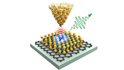
An electron “jumps” to the defect site
The two pulses are then sent to the STM and directed to the probe tip. The first pulse releases electrons from the tip, which “jump” to the location of the two-dimensional MoS defect2 layer and excite the electrons there.
“These could be electric charges, spin excitations, lattice vibrations, or the electron-hole pairs that we create there,” explains Schuler. “With the second pulse, we then see a few picoseconds later how our defect site responds to the excitation pulse and with that we can study the process of decoherence and energy transfer into the substrate.”
In this way, Schuler is one of the few specialists in the world to combine the short time resolution of picoseconds with a method that can “see” individual atoms. The team used the intrinsic localization of states in the 2D material system to hold excitations in one place long enough to be detected.
“Ultrafast lightwave scanning probe microscopy allows exciting new insights into quantum mechanical processes at the atomic scale, and 2D materials are a unique materials platform for creating these states in a controlled way,” said researcher Empa.
[ad_2]
Source link